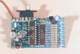
PCB Artwork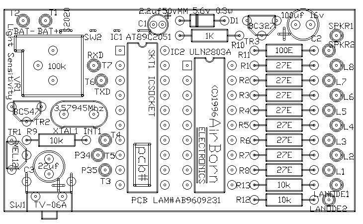
The PCB art, overlay, is pictured above. This image is a .GIF file saved at 300dpi. Most browsers can be instructed to download and save this image quite easily - for instance with Netscape, you right click on the image, then choose "save image as...". As the image is saved at 300dpi, a standard resolution of laser printers, you can print it out directly onto transparent film for making your own PCBs, and the scale will be substantially correct. The overlay diagram is used for the silkscreen (legend) of the circuit board 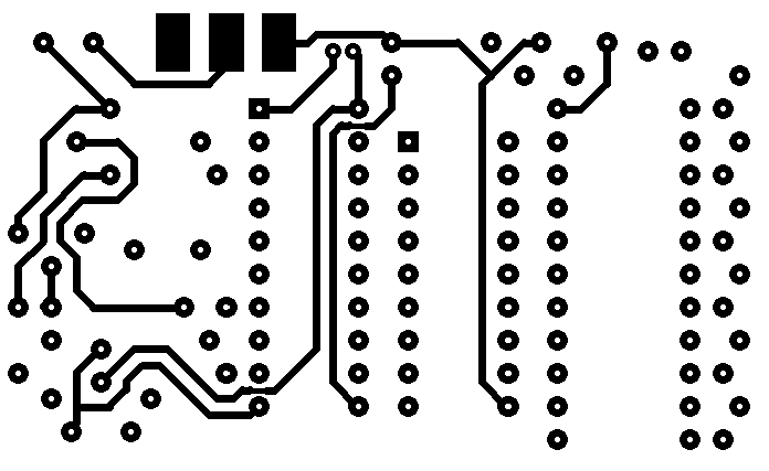
The PCB art, top layer, is pictured above.
The top layer diagram is used for the tracks that go on the component side of the circuit board. 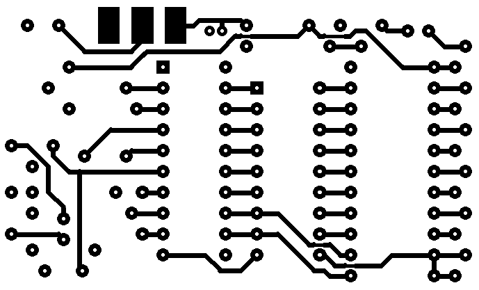
The PCB art, bottom layer, is pictured above. This image is a .GIF file saved at 300dpi. Most browsers can be instructed to download and save this image quite easily - for instance with netscape, you right click on the image, then choose "save image as...". As the image is saved at 300dpi, a standard resolution of laser printers, you can print it out directly onto transparent film for making your own PCBs, and the scale will be substantially correct. The bottom layer diagram is used for the tracks that go on the solder side of the circuit board. The layer is printed as if you are viewing through the circuit board (this is a convention used so that the layers line up) and will have to be reversed left-for-right before the copper tracks are printed.
HSETI PCB Art - Hole drilling diagramThe PCB art, hole drilling diagram, can be obtained through the above link. The hole diagram is also saved as 300 dpi, but is usually not used to make a to-scale diagram.
HSETI PCB Art - Protel format CAD fileThe PCB art, in protel CAD format, can be obtained through the above link. Parts ListHSETI1.PCB 19:51 10-9-1996 PCB Parts List A1 (C)1996 LOGO1 C1 2.2UF50VMM RB.06/.15 C2 100UF 16V RB.1/.2 C3 22UF RB.1/.2 D1 5.6V 0.3W DIODE0.3 IC1 AT89C2051 DIP20 IC2 ULN2803A DIP18 L1 TP L2 TP L3 TP L4 TP L5 TP L6 TP L7 TP L8 TP LANODE1 TP LANODE2 TP SPKR1 TP SPKR2 TP PCBLAM# AB9609231 PCLAMINATE R1 27E AXIAL0.4 R2 27E AXIAL0.4 R3 27E AXIAL0.4 R4 27E AXIAL0.4 R5 27E AXIAL0.4 R6 27E AXIAL0.4 R7 27E AXIAL0.4 R8 27E AXIAL0.4 R9 10K AXIAL0.4 R12 10K AXIAL0.4 R13 10K AXIAL0.4 R10 1K AXIAL0.4 R11 100E AXIAL0.4 SKT1 ICSOCKET DIP20 SW1 TV-06A TV-06A SW2 S2020 S2020SMT T1 BAT+ TP T2 BAT- TP T3 P35 TP T4 INT1 TP T5 P34 TP T6 TXD TP T7 RXD TP TR1 MEL12 TO-92A TR2 BC547 TO-92A TR3 BC327 TO-92A VR1 100K VR4 XTAL1 3.57945MHZ XTAL2 Total Components = 48 Parts description
Parts Notes
HSETI ProgrammingHSETI assembler test program (hseti.ASM)Assembler tools to compile hseti.asmThe program needed for the HSETI PCB will depend on what you want to do with the board. We have written a small skeleton program in 8051 assembler, the link for this is provided above. Also the assembler is available for download, the assembler is shareware, continued use will require registration.
The program HSETI.ASM, above, contains equates for the I/O and exercises all the port bits. Running it should allow you to quickly test your new HSETI board.
Using the HSETI PCB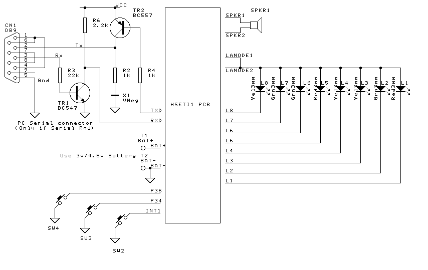
The diagram above shows a typical circuit using the HSETI PCB, with the optional serial port in place also. The serial port does not have strict RS232 level signals, but will work with just about all PC clones with reasonable cable lengths. The "component" X1 is just a link. To get better RS232 levels, cut X1 and insert a negative 3-4.5v power supply. This will give a +3/-3v RS232 Tx signal, which is better at driving longer cables than the +3v/0v signal obtained with X1 as a link.
As noted previously, while this diagram shows 3v/4.5v battery, for best results, use 4.5-5v, or omit ULN2803A.
This design is provided available for whoever wants it. There is no guarantee attached to it, naturally, although you can be assured that we have built the board as described, and run the test program on it. The original use for the board was for a kids group project here in NSW, Australia - making a "UFO" with flashing lights!
|