This example is intended to illustrate the technical documentation of an electronic design produced by AIRBORN ELECTRONICS. Most of the technical drawings in this page have been reduced in resolution so they can be viewed easily. The full sized diagrams may be downloaded from our circuit collection.All material contained in this document is Copyright ©2010 AirBorn Electronics.RCM710 ELECTRONIC SCALETechnical Design ManualRCM Weighing
Document Part 1RCM710 Interboard connector (CN15 Lead)DescriptionThe Lead is a 26 way 0.050 inch pitch ribbon cable, terminated at each end with 26 way IDC mini-female socket (bump or clip polarisation). Typical terminating connectors are type Fujitsu FCN747J026AU0.
Factory only adjustment #5DescriptionThe factory only adjustment number 5 trims the +5v rail to 5.12v. This is needed for correct operation of the 87C552 A/D converter. The remainder of the circuitry on the PCB is also sensitive to power supply voltage, and having a stable reference voltage will ensure satisfactory operation.
Trimming of this voltage to a voltage other than 5.12v could have an adverse effect on the operation of the RCM710 unit. The adjustment should only be made in the factory, with proper calibrated equipment.
Equipment
Procedure
TestsTest how far the 5.120v supply drifts with:
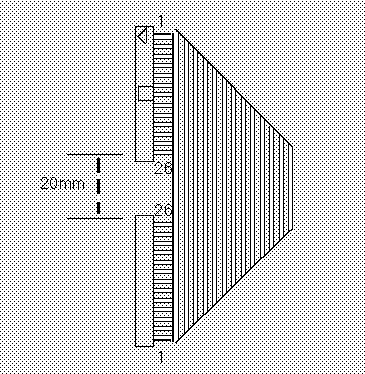
Provisional Transformer specification - Stage 4 Electronic Scale headwork5 November 1993Construction:
Winding:
Primary:
Secondaries
RCM710 Connector PinoutsCN1 - Transformer10 Way 0.2 inch pitch Weidmuller-Klippon SL10-H or wafer connector
CN2 - Primary Load Cell8 Way 0.2 inch pitch Weidmuller-Klippon SL8-H
CN3 - Bus COM's3 Way 0.2 inch pitch Weidmuller-Klippon SL3-H
CN4 - Feature connector8 Way 0.1 inch pitch posts
CN5 - Batcher connector8 Way 0.1 inch pitch posts
CN6 - Printer module connector6 Way 0.1 inch pitch posts
CN7 - Ancillary COM's module connector8 Way 0.1 inch pitch posts
CN8 - System COM's RS232 module connector8 Way 0.1 inch pitch posts
CN9 - I2C Connector A5 Way 0.1 inch pitch posts
CN10 - I2C Connector B5 Way 0.1 inch pitch posts
CN11 - Remote print switch4 Way 0.2 inch pitch Weidmuller-Klippon SL4-H
CN12 - Analog output connector4 Way 0.1 inch posts
CN13 - Chassis connectionSpade connector
CN16 - Vtest2 Way 0.1 inch posts
CN14 - Alternate Load Cell10 Way 0.1 inch posts
CN15 - Interboard connector (Display-Keyboard)26 Way 0.1 inch x 0.1 inch dual row Insulation Displacement Connector (Suitable example part number: PCB - Fujitsu FCN744P034AUR, Cable - FCN747B034AUO)
J1 - Load Cell Sensitivity3 Way 0.1 inch posts - short with 2 Way shunt
J2 - Programming Link3 Way 0.1 inch posts - short with 2 Way shunt Also used as special connector for "Dongle" operation
J2 - Dongle connector3 Way 0.1 inch posts Also used as Programming link when no Dongle present
J3 - RS485 Termination Link3 Way0.1 inch posts - short with 2 Way shunt
87C552 Pinout definitionRCM710 HeadworksPin Name Function 1 P5.0 In Analog input. Print Switch 2 Vdd +5v 3 STADC Gnd 4 *PWM0 Out Piezo. 0 = Voltage across Piezo element 5 *PWM1 Out Brightness. 0 = Fluro on, keyboard off 1 = fluro off, keyboard on 6 *EW Gnd 7 P4.0 Out Integrator select A: 0 = -Sig or DoRef 1 = Vdd/2 " " Upgood strobe. Strobes continuously during correct code operation. 8 P4.1 Out Integrator select B: 0 = DoRef 1 = -Sig or DoRef 9 P4.2 Out Fast fill relay. 0 = Operate relay 10 P4.3 Out Slow fill relay. 0 = Operate relay 11 P4.4 Out Diag LED 1: Green " " Force10v. 1 = Force excitation voltage to 10v instead of 12.5v 12 P4.5 Out Diag LED 2: Red " " ATest. 0 = Add analog test voltage into input circuitry 13 P4.6 Out RTSA. Direction control for RS485 port in system mode. 0 = Transmit " " DTRA. Handshake line for channel A (System) 0 = +12v output = active 14 P4.7 Out DTRB. Handshake line for channel B (Ancillary) 0 = +12v output = active 15 RST In Reset. Capacitor to +5v. When input is at +5v, processor is reset. 16 P1.0 In Settle. 0 = Discharging integrator capacitor. 1 = Integrating. 17 P1.1 In I2C interrupt input (Potentially unused) 0 = Interrupt " " In/Out Feature connector pin 1 18 P1.2 In/Out Feature connector pin 2 19 P1.3 In/Out Feature connector pin 3 20 P1.4 In CTSA. Handshake line for channel A (System). 0 = +12v = active: ok to send data on TxDA 21 P1.5 In CTSB. Handshake line for channel B (Ancill). 0 = +12v = active: ok to send data on TxDB 22 P1.6 In/Out SCL. I2C clock line. 23 P1.7 In/Out SDA. I2C data line. 24 P3.0 In RxDA. Serial Receive line for channel A (System). 0 = +12v = space, active data condition. 25 P3.1 Out TxDA. Serial Transmit line for channel A (System). 0 = +12v = space, active data condition. 26 P3.2 In RxDB. Serial Receive line for channel B (Ancill). 0 = +12v = space, active data condition. 27 P3.3 In IRRx. Demodulated carrier. 0 = active 38khz carrier present. 28 P3.4 Out TxDB. Serial Transmit line for channel B (Ancill). 0 = +12v = space, active data condition. 29 P3.5 Out GagSel. Gauge select signal. 1 = Standard gauge 0 = Alternative (#2) gauge 30 P3.6 Out Fluro Segment 8. 1 = active, when a grid is active. Note all segments go to '1' briefly at reset. 31 P3.7 Out Fluro Segment 9. 32 nc no connection 33 nc no connection 34 XTAL2 Crystal connection 35 XTAL1 Crystal connection 36 Vss Gnd 37 Vss Gnd 38 nc no connection 39 P2.0 Out Scan0. Scan0-Scan3 together select a fluro display grid to turn on, and/or a keybd line to scan. 40 P2.1 Out Scan1. 41 P2.2 Out Scan2. 42 P2.3 Out Scan3. 43 P2.4 Out Printer module connector pin 1. PDatOut 44 P2.5 Out Printer module connector pin 2. PClk. Positive transition = latch valid data on PDatOut 45 P2.6 Out Printer module connector pin 3. PLoad. 0 = active 1 = inactive. " " Out Strobe. 0 = active, as long as PDatOut is also 0. 46 P2.7 In Printer module connector pin 4. PDatIn. Changed on Positive transition of PClk. 47 *PSEN Out Unused. Should be permanently high. 48 ALE/ *PROG Unused. Should be an active high pulse at 1/6th of the crystal frequency. 49 *EA/Vpp +5v 50 P0.7 Out Fluro Segment 7. 1 = active, when a grid is active. Note all segments go to '1' briefly at reset. " " In Keyboard return 7. 0 = active, when an appropriate keyboard scan line is selected. 51 P0.6 Out Fluro Segment 6. 1 = active. " " In Keyboard return 6. 0 = active. 52 P0.5 Out Fluro Segment 5. 1 = active. " " In Keyboard return 5. 0 = active. 53 P0.4 Out Fluro Segment 4. 1 = active. " " In Keyboard return 4. 0 = active. 54 P0.3 Out Fluro Segment 3. 1 = active. " " In Keyboard return 3. 0 = active. 55 P0.2 Out Fluro Segment 2. 1 = active. " " In Keyboard return 2. 0 = active. 56 P0.1 Out Fluro Segment 1. 1 = active. " " In Keyboard return 1. 0 = active. 57 P0.0 Out Fluro Segment 0. 1 = active. " " In Keyboard return 0. 0 = active. 58 AVref- Gnd 59 AVref+ +5v. For purposes of this pin the +5v supply is actually trimmed to 5.120v. 60 AVss Gnd 61 AVdd +5v 62 P5.7 In Analog input. IOut. Test diagnostic line to monitor integrator output voltage, divided by 4. 63 P5.6 In Analog input. RawAnout. Test diagnostic line to monitor raw analog signal, divided by 4. 64 P5.5 In Analog input. +Excite. Test diagnostic line to monitor Bridge excitation voltage, divided by 4. 65 P5.4 In Analog input. Potentiometer input. 66 P5.3 In Analog input. Program mode - Revision level link on Keyboard-display PCB. 67 P5.2 In Analog input. Light dependent resistor. 68 P5.1 In Analog input. NTC thermistor, for temperature measurement.
Drilling Diagram: RCM710 CPU Board[Full resolution diagrams can be viewed in the circuit collection]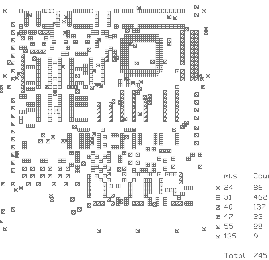
Overlay Diagram: RCM710 CPU Board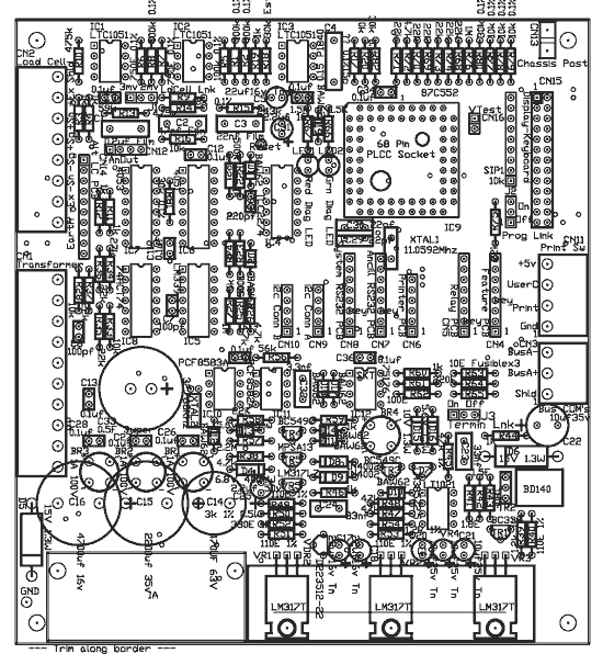
Circuit Diagram: Keyboard/Display PCB 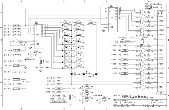
RCM2_1.PCB  1:51  25-8-1996       PCB Parts List

A1                                                     LOGO1
CN15               RCM710 HEADWORKS PCB                IDC26
D1                 BAW62                               DIODE0.3
D2                 BAW62                               DIODE0.3
D3                 BAW62                               DIODE0.3
DISP1              FIP6A13A                            FIP6A13A
IC1                4051                                DIP16
IC2                4051                                DIP16
IC3                SA594                               DIP18
IC4                SA594                               DIP18
IC5                74HCT04                             DIP14
PZ1                PIEZO                               RB.4/.8
R1                 27K                                 AXIAL0.4
R2                 10K                                 AXIAL0.4
R3                 10K                                 AXIAL0.4
S1                 KEY:1                               KEY-SW
S2                 KEY:2                               KEY-SW
S3                 KEY:3                               KEY-SW
S4                 KEY:4                               KEY-SW
S5                 KEY:5                               KEY-SW
S6                 KEY:6                               KEY-SW
S7                 KEY:7                               KEY-SW
S8                 KEY:8                               KEY-SW
S9                 KEY:9                               KEY-SW
S10                KEY:0                               KEY-SW
S11                KEY:TARE                            KEY-SW
S12                KEY:FIX                             KEY-SW
S13                KEY:CLR                             KEY-SW
S14                KEY:SUB                             KEY-SW
S15                KEY:PRINT                           KEY-SW
S16                KEY:FEED                            KEY-SW
S17                KEY:ZERO                            KEY-SW
Total Components = 32
Drilling Diagram: RCM710 Keyboard/Display Board[Apologies: Poor resolution is the result of scaling to fit page format][Full resolution diagrams can be viewed in the circuit collection] 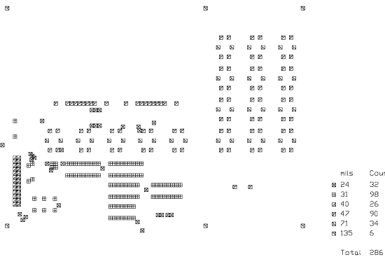
Overlay Diagram: RCM710 CPU Keyboard/Display Board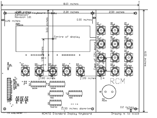
Overlay Diagram: RCM710 CPU Board: ColourThis diagram is not normally included in the technical documentation package, because of difficulties in reproduction.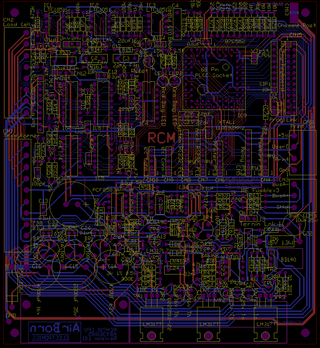
|