Reliable Custom Design Click here to contact AirBorn
 
--AirBorn Electronics-- US SITE · AUS SITE
ABOUT US
Company Detail
Enquiry Form
Sitemap
WHAT WE MAKE
Our Design method
Spec'ing your job
Hardware design
Firmware design
Examples: Circuits
Subject Overview     Next Subject     Exit Site
Example projects
OUR CIRCUITS
Mechatronic controller
Programmable oscillator
RS485 firepanel int
IRDA Interface
Nursecall indicator
Serial to Parallel
Navy SMD Trainer
Danfoss tester
89C2051 project
Weighscale
Light Key Tone Gen
Index - Main Library
OUR DESIGN STEPS
Design step-by-step
Circuit diagrams
PCB Layout
PCB Etching
Prototyping
Firmware design
Documentation
Manufacturing
Economies of scale
Test Procedures
ECOs - changes
SPECIFY YOUR WORK
Overview
Specification Intro.
Writing a Spec
Tech Ingredients
Example Specs
Engineer employment
R&D Economics
Design Inspiration
REFERENCE
Autotrax PCB CAD
Autotrax resources
Autotrax utilities
Protel VESA drivers
Products - 1990s
Our PicoBus IO Std
RS232 RS485 FR4 Autotrax CAD Library P89LPC932 Program Header
Using a Multimeter
FURTHER INFO
Complete site index
Offsite Links (15000+)
Google search
 
--AirBorn Electronics-- CONTACT or ENQUIRY
©2010 AirBorn

Picobus - timing information

This page expands on our basic picobus information page, by illustrating the timing of the bus.

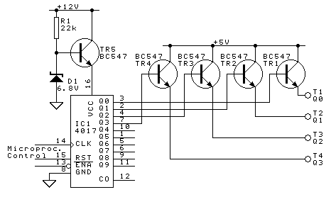
Typically the "Qn" timing on the Picobus will be handled by the scanning microprocessor. The scanning microprocessor may generate the Q0/Q1/Q2/Q3 signals directly, but more likely there will be an external counter or decoder run by the microprocessor. While only 4 lines are shown on picobus, the timing allows for up to 10 multiplexed signals total. A typical circuit is below:

Note: This circuit is presented as a typical example only and is not mandatory
PicoBus multiplex generator circuit
Typical PicoBus multiplex generator circuit

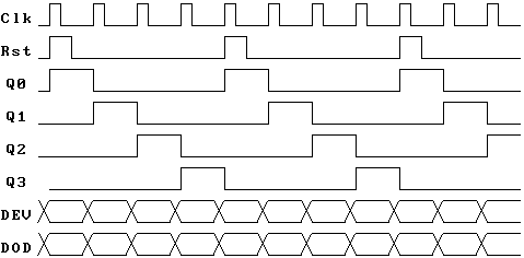
The typical timing involves the microprocessor issuing a clock pulse once every multiplex period. Most implementations will have the Reset signal pulsed once every 'n' multiplex periods. The data being sent out to multiplex devices (as distinct from the data being read back from these devices) is changed just prior to the new clock edge. For this reason, it is most suitable to have some port lines (for instance and preferentially DEV) as outputs, and others (for instance and preferentially DOD) as inputs if required. A typical timing diagram is shown below.

PicoBus multiplex timing
Typical PicoBus multiplex timing Magnified detail

One of the real advantages of Picobus, is that even though it includes power, ground, and i2c signals, the multiplexing leaves enough signals available so that "8 wide" devices such a DIP-switch can still be connected.
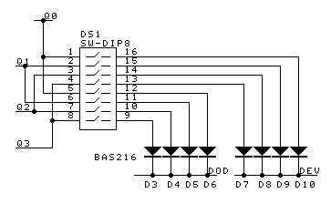
8 way dipswitch example circuit


This page had a Maintenance update: 23 April 2013

Subject Overview Subject Continue