Pressure Sensor
|
 |
|||||||||||||||||||
| Client |
 J Dickens |
|||||||||||||||||||
| Project (Short name: psensor) |
Pressure Sensor |
|||||||||||||||||||
| Project Status |
Design work Complete |
|||||||||||||||||||
| PCB Number |
AB0402235 |
|||||||||||||||||||
| Version Date |
24 Feb 2004 |
|||||||||||||||||||

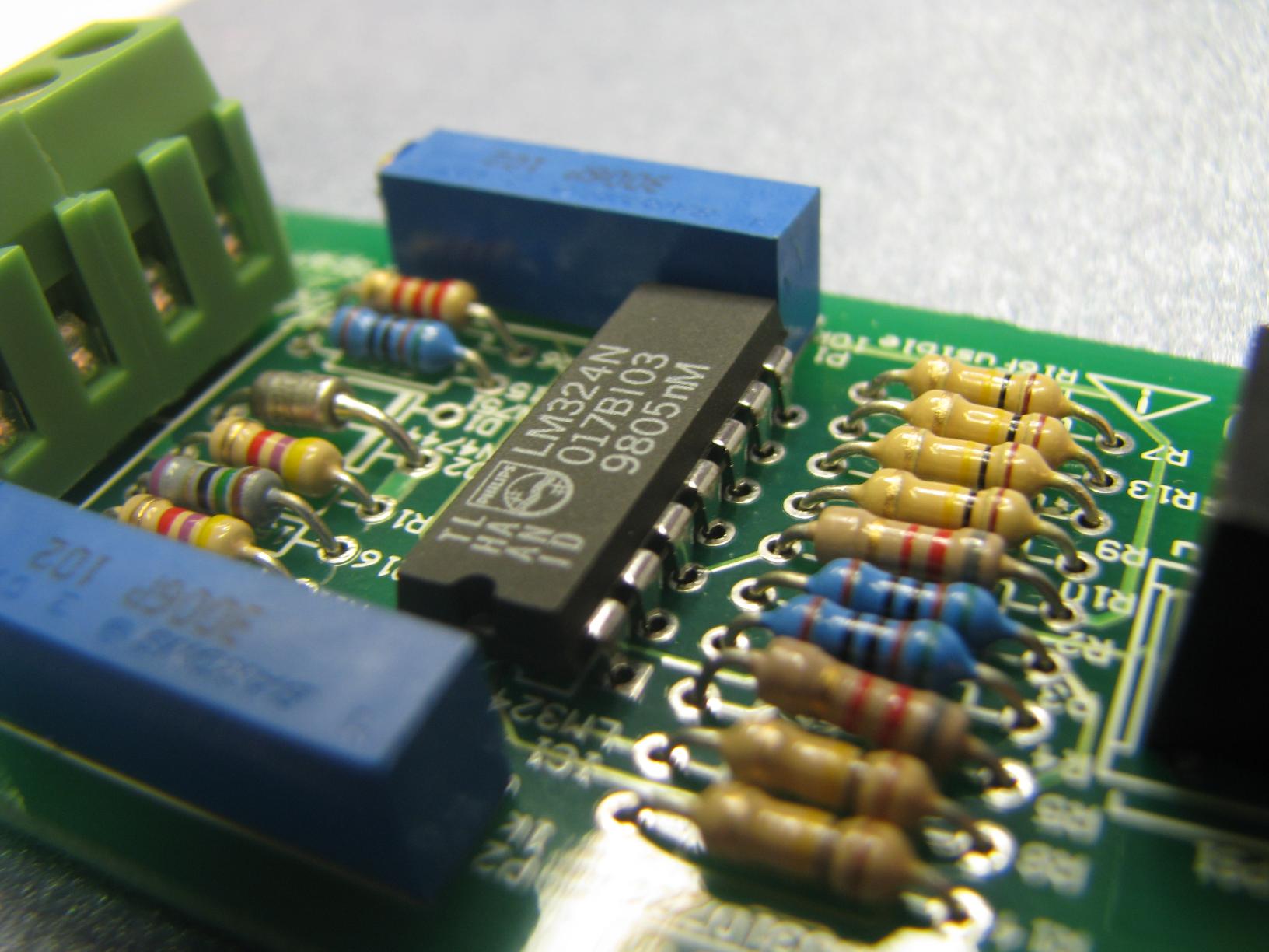
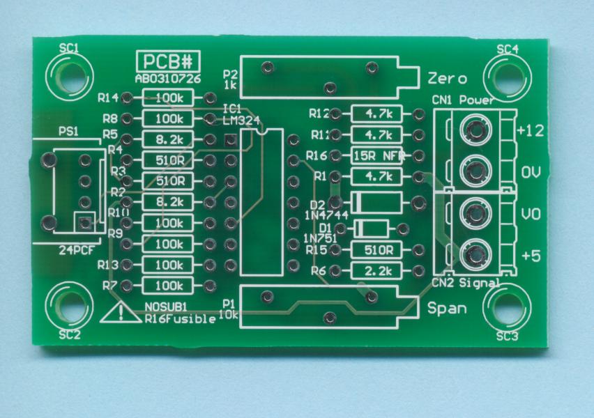
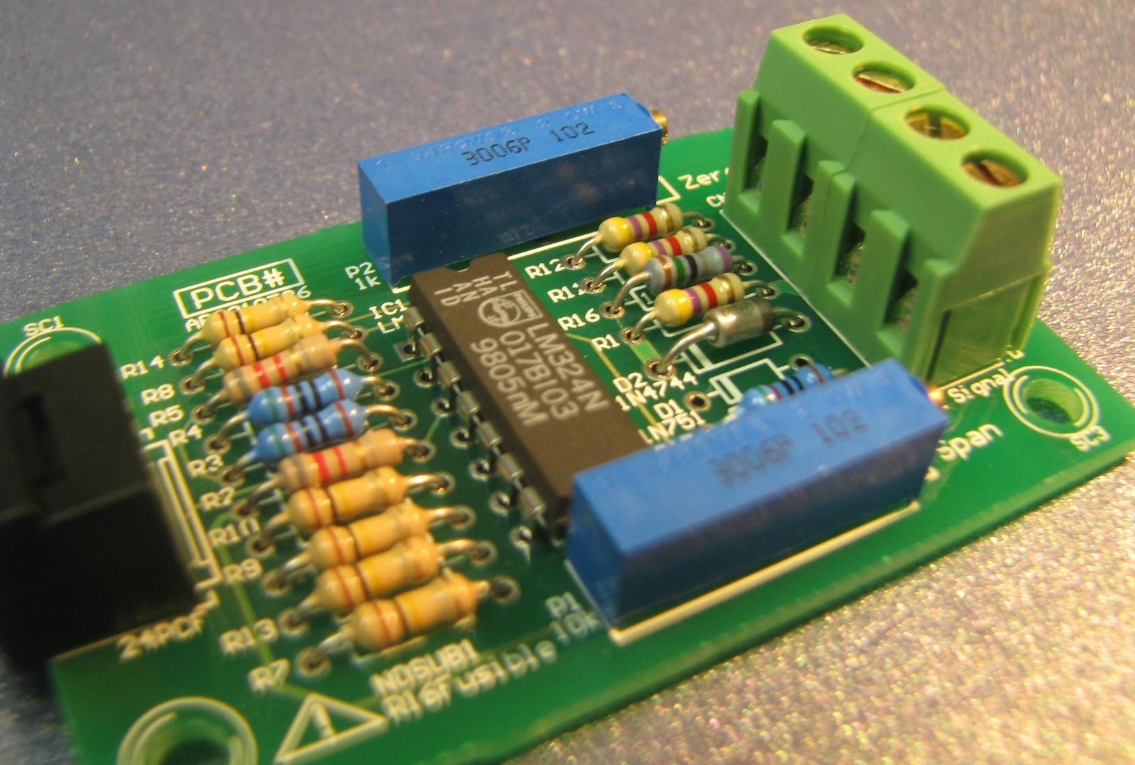
Circuit DiagramThe brief with this project was to produce cost effective electronics that could be assembled by a small, informal PCB manufacturing plant based in India, repaired easily, and producible with the minimum of setup. As such we designed the PCB to use conventional components (that is, Thru-Hole) rather than surface mount. We used straight forward design techniques and the most common components that we could. This circuit board is designed to be mounted remotely (by a meter or two) from the CPU board and conditions the low level signal from a pressure sensor for transmission to, and A/D conversion at, the main board. A pressure sensor needs a stable excitation voltage for reliable readings, this can either be the main board +5V supply - which also gives the advantage of providing readings ratiometric to the A/D reference voltage - or if desired a local zener reference can be fitted. A plain vanilla LM324 op-amp provides the excitation drive (IC1:A) and the conditioning in a standard three-op-amp instrumentation amplifier (Reference: Horowitz and Hill, the Art of Electronics, 2nd Ed, 7.10). The standard circuit has been modified to achieve zero and span adjustment based on the same excitation voltage used for the pressure sensor. The circuit is completed with a little power supply protection in the form of D2 and R16. R16 will open if the power supply is reveresed or goes overvoltage, hopefully protecting the rest of the circuitry. The board is fairly compact, with the Span and Zero multiturn adjustment pots flanking each side of the main board, the four wiring block connectors at one end, and the pressure sensor at the other.
|
||||||||||||||||||||
Bill of materials
Parts list and notes |
Pressure Sensor Bill Of Materials |
|||||||||||||||||||
PCB design
|
 |
|||||||||||||||||||
Gerber files
The PCB manufacturing files |
Pressure Sensor Gerber files |
|||||||||||||||||||
Final board |
 |
|||||||||||||||||||
 |
||||||||||||||||||||
Documentation package |
Pressure Sensor Documentation (PDF) |
|||||||||||||||||||
| Copyright |
©2010 AirBorn Electronics Pty Ltd |
|||||||||||||||||||
- Contact Us
- Enquiry Form
- Sitemap
- Our Design method
- Spec'ing your job
- Hardware design
- Firmware design
- Examples: Circuits
- Examples: Photos
- Index of Client PCBs
- This page on website
- Our Circuit Library
- Serial to Parallel
- Navy SMD Trainer
- Danfoss tester
- 89C2051 project
- Weighscale
- Light Key
- Tone Gen
- Design step-by-step
- Circuit diagrams
- PCB Layout
- PCB Etching
- Prototyping
- Firmware design
- Documentation
- Manufacturing
- Economies of scale
- Test Procedures
- ECOs - changes
- Project Specifications
- Specification Intro.
- Writing a Spec
- Tech Ingredients
- Example Specs
- Engineer employment
- R&D Economics
- Design Inspiration
- Example projects
- ...more
- ...more
- A PCB Factory
- A real design Lab
- Our PicoBus IO Std
- RS232 RS485
- FR4
- Autotrax
- CAD Library
- P89LPC932
- Program Header
- Past products
- Using a Multimeter
- Complete site index
- Offsite Links (15000+)
- Google search
- Contact
©2010 AirBorn - Last updated 08 July 2010
Background Image Credit: Dust Pillar of the Carina Nebula: NASA, ESA, and M. Livio and the Hubble 20th Anniversary Team (STScI)