Test Procedures for new Designs
The counterpoint to a specification is a test procedure. With a specification and an incoming test procedure, a client can have assurance that he gets what he orders.
There are actually three types of test procedures we are concerned with here
- Debug Test procedure - developed by the engineer to debug the design
- Incoming Test procedure - developed by Client to check delivery of the design work
- Manufacturing Test procedure - developed by the Manufacturer to test units as they are produced
Debug Test procedure
The debug test procedure will be developed by the design engineer as the design proceeds. If he does not do this, he is either overconfident, unaware, or very pushed for time. (A cynical meme: Overconfident engineers do not stay hands-on-tools for long, as they keep making mistakes. Very soon they learn to become managers, so they will have someone else to blame for the project failures!)
The aim of the debug test procedure is to divide the testing of the design into small, autonomous units. In this respect the debug test is providing a tool for the detection of faults in the design in a way that most conveniently allows them to be fixed - by finding them in isolation.
The debug test procedure will pay particular attention to suspected trouble spots in a design. For instance, if an analog input is known to be operating at a particularly low input signal level, a debug test procedure might include noise measurement, thermal drift testing, and evaluation of potential cross talk sources.
Some bugs are really difficult to pin down. The worst types are the intermittent bugs - bugs which do not seem to have a correlation with a known condition, and perhaps occur rarely. The best approach is methodical, documented work. As each test is performed, it should be written down in a log. While the pressure may be on, the designer will need time to solve these, and time to think about what to do next. Frequently there actually may be a correlation with some outside event - EMI, timing, a certain operation, or a spike through the power. Being methodical and recording everything may pin it down.
If the designer has time to develop the test procedure as the design proceeds (rather than as an afterthought) they can add test points to the board, and make it easier to divide up the circuitry at the prototyping stage. Dividing the circuitry can be done with jumpers (but honestly, there is rarely enough space) or by removing a component - perahps a 0 ohm resistor inserted for the purpose - or, most usually, by cutting a track (and doing a reasonable repair afterwards). If the designer has time to think all this through before sending the board off for manufacture, they can ensure that the critical connecting tracks are not, for instance, under an IC or on an internal layer where they cannot be easily cut.
The debug test procedure will normally also include an overall functional test, based on the specification. This is basically equivalent to the incoming test procedure applied by the client. If a client is dealing with an open, trustworthy and thorough designer they may actually be able to avoid doing the incoming test themselves. The designer should explain to the client at handover the details of any functional testing carried out. That way the client has a starting point for their own testing of the prototypes, and it also avoids a potential disaster: If a client applies different incoming tests to the designers overall functional test, the clients test may fail, while the designers test passes. Atleast if the designer was straightforward in telling the customer what and how they tested, the customer may accept that a different test may reveal an undiscovered bug.
Incoming Test procedure
The clients incoming test procedure will normally start with the specification of the product and test that the specified features are actually delivered. This testing may be a repeat of part of the overall functional test procedure carried out by Design engineer. Handover should be used as an opportunity for the designer to demonstrate the prototype to the client, ticking off as many of the Incoming test procedure items as possible, and covering the remainder verbally.
The incoming test procedure has different objectives from the debug test procedure - its aim is to prove that the design meets the specification. Overall tests are usually good for this objective. The debug test procedure is attempting to isolate any faults in the design. This requires testing by section and thorough characterisation of the design rather than just meet spec/miss spec results. Having said that, every design misses a spec somehow. The key is to minimise the impact - have a workaround, or a fix in progress, or at least have documented how and why the target was missed.
Specification "bugs". Sometimes the designer and client have different interpretations of the design requirements. The designer may build a prototype which misses a feature required by the client. The most efficient way around this is communication during the design process - but in lieu of this, at least the problem is discovered at the prototype stage, not manufacture. How it is resolved by the two parties is a compromise - the designer did not quote on the feature, and the client expected the feature to be in the quote - a commercial compromise is needed by one or both parties.
Manufacturing Test procedure
The manufacturing test procedure is used to test product as it is being manufactured. The procedure is quite dependent on the manufacturer, his production techniques, and his testing equipment. At a minimum the manufacturer will need a production sample from the client. The manufacturing test procedure is an economics driven test. The procedure is designed to save money for the manufacturer. We suggest reputation is also an attribute that can be priced, hence the statement.
For instance, depending on the application of the equipment, it would be possible
to deliver all circuitry completely untested, and indeed this is the aim of many
ISO9000 manufacturing flows. However, any failures would incur a financial cost,
both in terms of returns, rework & replacement, and also the manufacturer / client
reputation.
At the extremes: a cheap toy, or superlative manufacturing with very few defects
(six sigma), no testing is an option. The aim, otherwise, is to find a manufacturing
test procedure which reduces the outgoing failure rate while not costing more than it saves.
- There are four basic types of "testing", in order of capital expenditure:
- Visual Inspection Its simple, its cheap, and everyone should do it.
Having a skilled person inspect the PCBs will find most of the faults.
For one or two units in the manufacturing run the visual should be pretty
exhaustive, checking every component against the equivalent on the production
sample and BOM, and questioning even if the logo on an IC looks different.
Visual inspection for the bulk of the manufacturing run is a quick process looking for orientation, solder defects and ensuring the correct parts are in the correct place. A visual also weeds out badly produced but operational boards - for instance where thru-hole parts are improperly seated before soldering - Operational Test (Sometimes called Go/Nogo) With appropriate firmware, powering up a board will test a fair amount of circuitry even without a test jig. The response can be compared to the production sample.
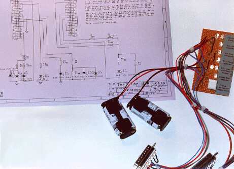
- Test Jig This is a standard test method. A Jig is made that plugs into the
PCB to be tested, and exercises the inputs and outputs. Often the test is more
functional than parametric - that is, it does not attempt to test if an output
can deliver full power for instance. A test jig finds most faults, and finds
them quickly. Test jigs are normally not expensive in unit cost, so it is
possible to make one for the client as well as one or more for the manufacturer.
 However, test jigs are quite expensive in terms of engineering time to develop.
Given current technology and the sorts of example boards on the AirBorn website,
it is our rough estimate that a test jig will cost 8-12% of the cost that it
took to develop the original PCB. Test jigs are normally not factored into the
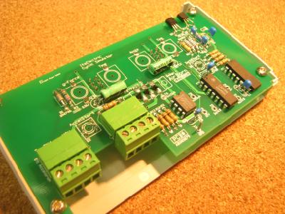
development cost. Two different test jigs are shown here - the one above is an
older type, hand built (but works just as well). The one to the right is built
on a circuit board - so more than one could be made easily.
However, test jigs are quite expensive in terms of engineering time to develop.
Given current technology and the sorts of example boards on the AirBorn website,
it is our rough estimate that a test jig will cost 8-12% of the cost that it
took to develop the original PCB. Test jigs are normally not factored into the
development cost. Two different test jigs are shown here - the one above is an
older type, hand built (but works just as well). The one to the right is built
on a circuit board - so more than one could be made easily. - Automated Test Equipment (ATE) This is the best test method. ATE will have pin drivers that can exercise inputs and load outputs to do parametric testing in addition to functional testing. ATE will also be made to probe connections inside the circuit under test using a bed of nails. ATE is not cheap, and jigs and the programming for the equipment are an ongoing cost, but it is superior to a plain functional test. It is really quite difficult for a fault to get past a well constructed ATE test.
- Contact Us
- Enquiry Form
- Sitemap
- The PCB design method
- About Circuit diagrams
- About PCB layout
- About Firmware design
- Spec'ing your job
- Our design service
- Example Projects Library
- Mechatronic control unit
- Garbage truck compactor
- RS232-RS485 convert (2006)
- Tone generator test project
- RS485 fire panel int.
- Front panel switches( A/D)
- Serial to IRDA
- Danfoss loop tester
- RAN Multilayer trainer
- Programmable Oscillator
- Pressure sense PCB
- Nursecall overdoor light V2
- Design step-by-step
- Circuit diagrams
- PCB Layout
- PCB Etching
- Prototyping
- Firmware design
- Documentation
- Manufacturing
- Economies of scale
- Test Procedures
- ECOs - changes
- EMI & ESD in design
- FR4 and fire resistance
- Project Specifications
- Specification Intro.
- Writing a Spec
- Tech Ingredients
- Example Specs (older)
- Selecting a designer
- R&D Economics
- Design Inspiration
- Autotrax Utitilities
- Autotrax links
- Our PicoBus IO Std
- RS232 connectors
- Our RS485 converter
- P89LPC932
- Our Program header
- How to use a Multimeter
- Our Site index
- Offsite Links (15000+)
- Google search
- Contact
©2013 AirBorn - Last updated 01 May 2013