Designing PCBs for ESD and EMI compliance
One of the testing tasks that faces every PCB designer is designing for ESD and EMI compliance. An autorouter can only take a netlist and produces a set of connections - that does not actually help at all with EMI and ESD. It is up to the PCB designer to design the board so that it complies.
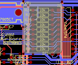
An important concept in PCB design for EMI compliance is loop area. A closed circuit of tracks, as shown in the illustration, comprises a loop. In simple terms: Interference can both exit and enter the PCB into areas inside loops. The smaller the dimensions of each loop, the smaller the magnitude of interference to be dealt with. The circuitry on the board will be contained inside several small loops, through having a gridded power supply distribution. The best distribution of the lot is one or two continuous planes or sheets of copper.
A four layer circuit board, with the two center layers being power and ground, is often used to minimize EMI emissions and susceptibility. One way this works is by making the loop area very small. When using double sided PCBs, without the opportunity for ground planes, special attention must be paid to loop area. 4 layer boards usually cost twice as much as double sided boards. There are situations where it is very desirable to use lower cost boards - double sided PCBs can often be made to perform quite satisfactorily with careful PCB design.
When the only tool you own is a hammer, every problem begins to resemble
a nail -- Abraham Maslow![]()
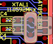
High frequency circuits, such as crystals, should be enclosed by an overall ground. If there is an opportunity to earth the metal case of such devices, it is usually worthwhile. The illustration shows a microprocessor crystal circuit, with the loading capacitors, and its overall shield track. With PCB layout like this, and careful supply routing and bypassing, a single chip microprocessor circuit board can often pass EMI emission tests on just a double sided PCB with no case shielding. The overall shield is also desirable on low level analog circuitry - in that situation it reduces interference reaching the low level circuitry
Input/Output lines to a circuit board can be subjected to extraneous voltage induced
or directly connected - such as Electrostatic discharge (ESD).
 The circuitry itself should be designed to withstand the voltage, - special components are
available to do this. It is also possible to supplement the protection with PCB spark gaps.
The spark gap shown here is manufactured to a common PCB tolerance - it is an 8 thou gap.
The contact area needs to be free of solder resist, in order to function as a sparkgap.
Breakdown of small sparkgaps is approx V=(3000pd+1350) where p is pressure in atmospheres
(1) and d is distance in millimetres. This sparkgap can be expected to have a peak voltage
of about 2000-2500V.
The circuitry itself should be designed to withstand the voltage, - special components are
available to do this. It is also possible to supplement the protection with PCB spark gaps.
The spark gap shown here is manufactured to a common PCB tolerance - it is an 8 thou gap.
The contact area needs to be free of solder resist, in order to function as a sparkgap.
Breakdown of small sparkgaps is approx V=(3000pd+1350) where p is pressure in atmospheres
(1) and d is distance in millimetres. This sparkgap can be expected to have a peak voltage
of about 2000-2500V.
Earthing of connector grounds and such lines as sparkgaps requires special consideration. Usually the best physical arrangement for these type of earth is the Star - where the earth happens at one place, and the lines go back to that place seperately. The most important issue is to carefully consider how the currents will flow to earth, especially under conditions of fault (for instance when one of the sparkgaps shown above is arcing over). The inductance and resistance of tracks and wires will cause voltage to be induced in the earth returns, and it is important to consider where these voltages will appear to avoid other circuitry malfunctioning or even being destoyed. Some very good texts on the subject start with the statement "There is no such thing as Ground" - that is probably the best simple advice to remember, - model every return path, don't accept that any point is necessarily "ground potential".
Whether you think you can or you think you can't,
you are usually right. -- Henry Ford (1863-1947)
![]()
- Contact Us
- Enquiry Form
- Sitemap
- The PCB design method
- About Circuit diagrams
- About PCB layout
- About Firmware design
- Spec'ing your job
- Our design service
- Example Projects Library
- Mechatronic control unit
- Garbage truck compactor
- RS232-RS485 convert (2006)
- Tone generator test project
- RS485 fire panel int.
- Front panel switches( A/D)
- Serial to IRDA
- Danfoss loop tester
- RAN Multilayer trainer
- Programmable Oscillator
- Pressure sense PCB
- Nursecall overdoor light V2
- Design step-by-step
- Circuit diagrams
- PCB Layout
- PCB Etching
- Prototyping
- Firmware design
- Documentation
- Manufacturing
- Economies of scale
- Test Procedures
- ECOs - changes
- EMI & ESD in design
- FR4 and fire resistance
- Project Specifications
- Specification Intro.
- Writing a Spec
- Tech Ingredients
- Example Specs (older)
- Selecting a designer
- R&D Economics
- Design Inspiration
- Autotrax Utitilities
- Autotrax links
- Our PicoBus IO Std
- RS232 connectors
- Our RS485 converter
- P89LPC932
- Our Program header
- How to use a Multimeter
- Our Site index
- Offsite Links (15000+)
- Google search
- Contact
©2013 AirBorn - Last updated 01 May 2013